Electronics Production and Design
ISP Programmer
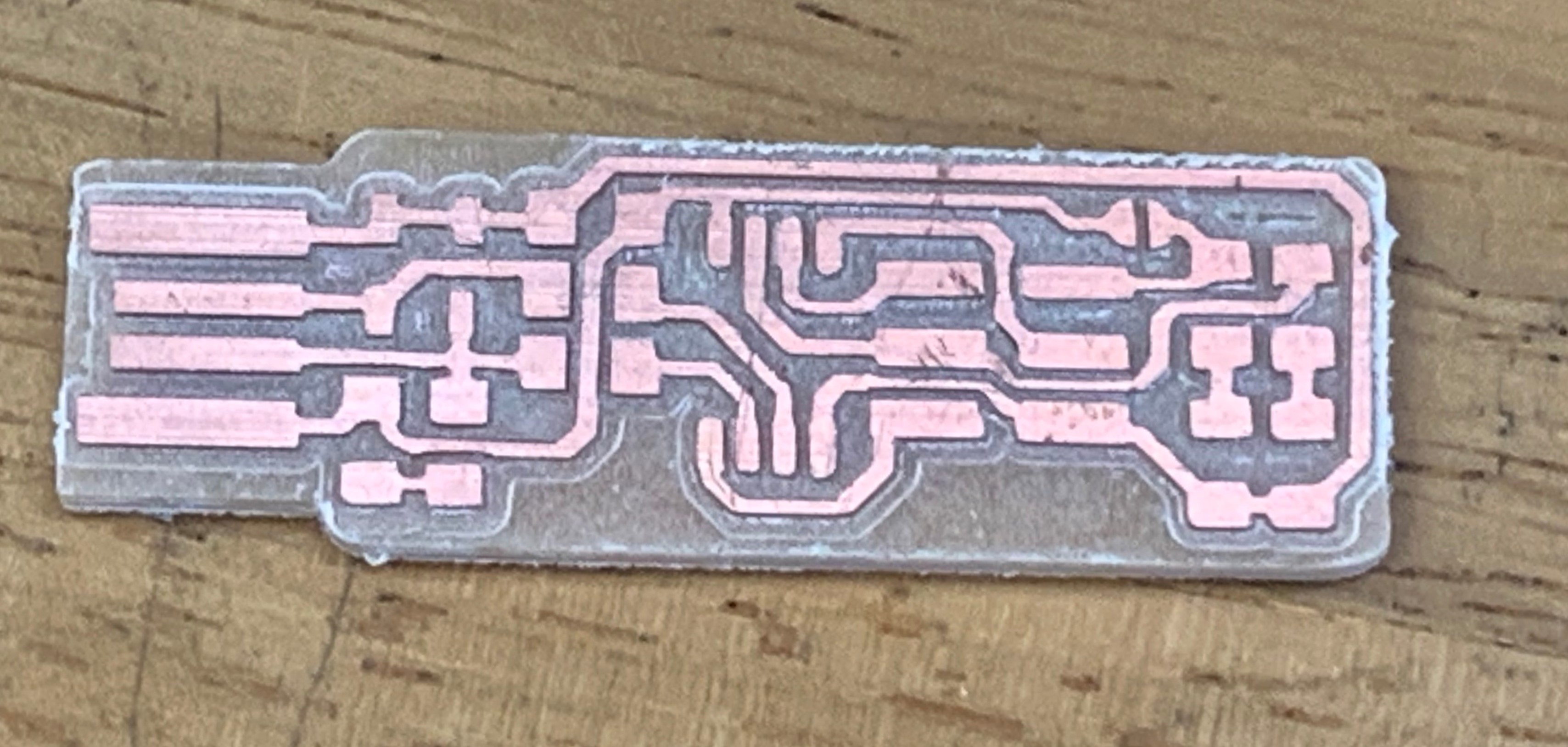
In this part of the module, we were tasked to make a im-circuit programmer by milling and stuffing the Printed Circuit Board and test it. We were provided an example ISP PSB design from our lecturer. One image was of the traces of the ISP and the other was of the outline of PCB.
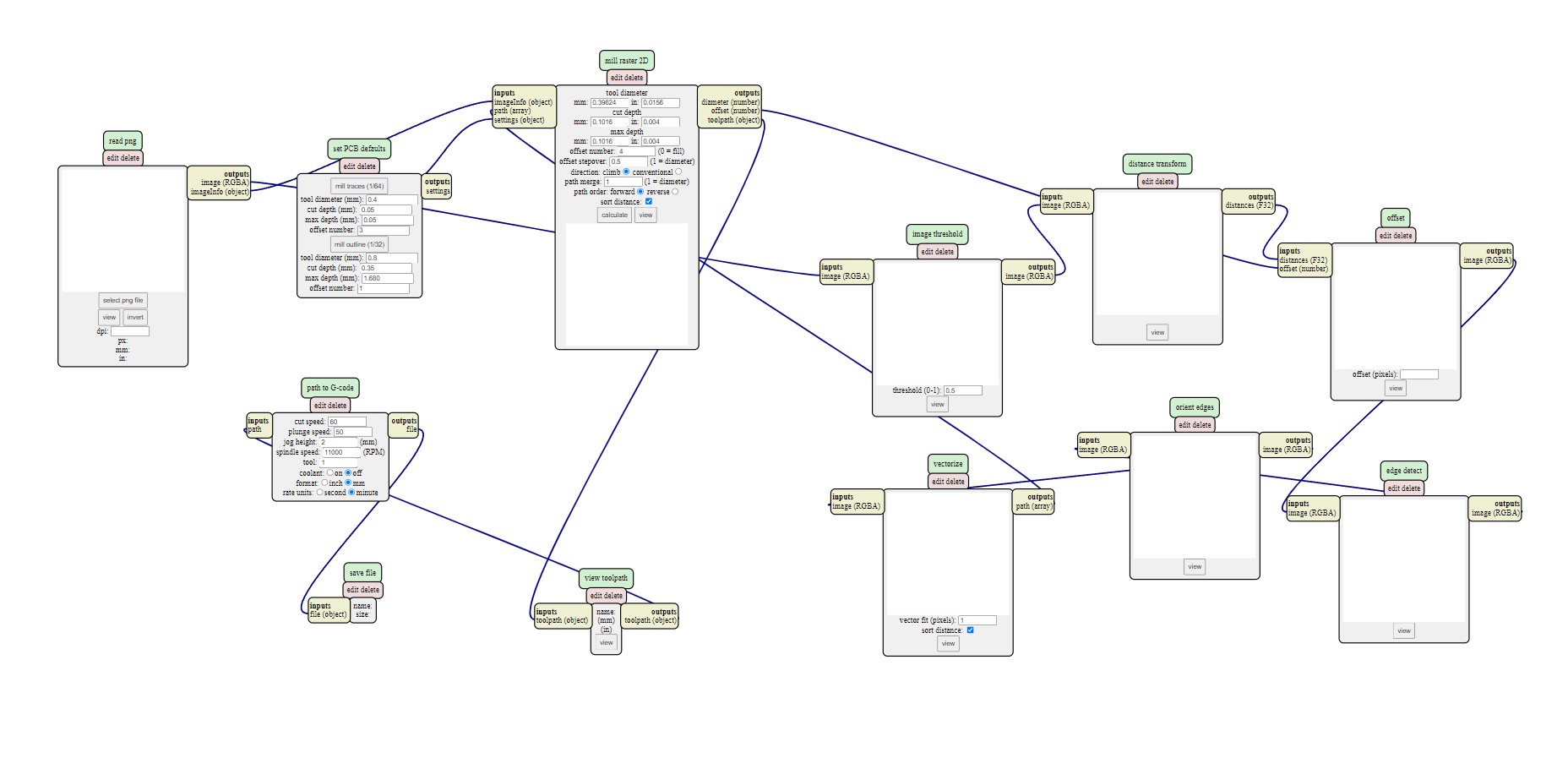
Once we acquired the pictures, we had to generate the gcode of the PCB from mods, a website that our lecturer provided. To open the program, you rightclick -> programs -> open server program -> (Under G-code) mill 2D PCB PNG. This interface should pop up on your screen.
The CNC machine we were using to mill the PCBs was the Stepcraft 420. As different machines require different settings, we had to set the different properties to specific values according to this table.
| Operation | Endmill Size | Cut Speed | Cut Depth | Total Depth | Offset |
|---|---|---|---|---|---|
| Traces | 0.1 mm 30 deg V-bit | 50~60mm/min | 0.04 ~ 0.05 mm | 0.04 ~ 0.05 mm | 1-2 |
| Board Outline | 0.8 mm flat | 50~60 mm/min | 0.42-0.45 mm | 1.65 ~ 1.70 mm | 1 |
These settings are subject to change depending on the endmill that is being used or the type of PCB that is being milled.
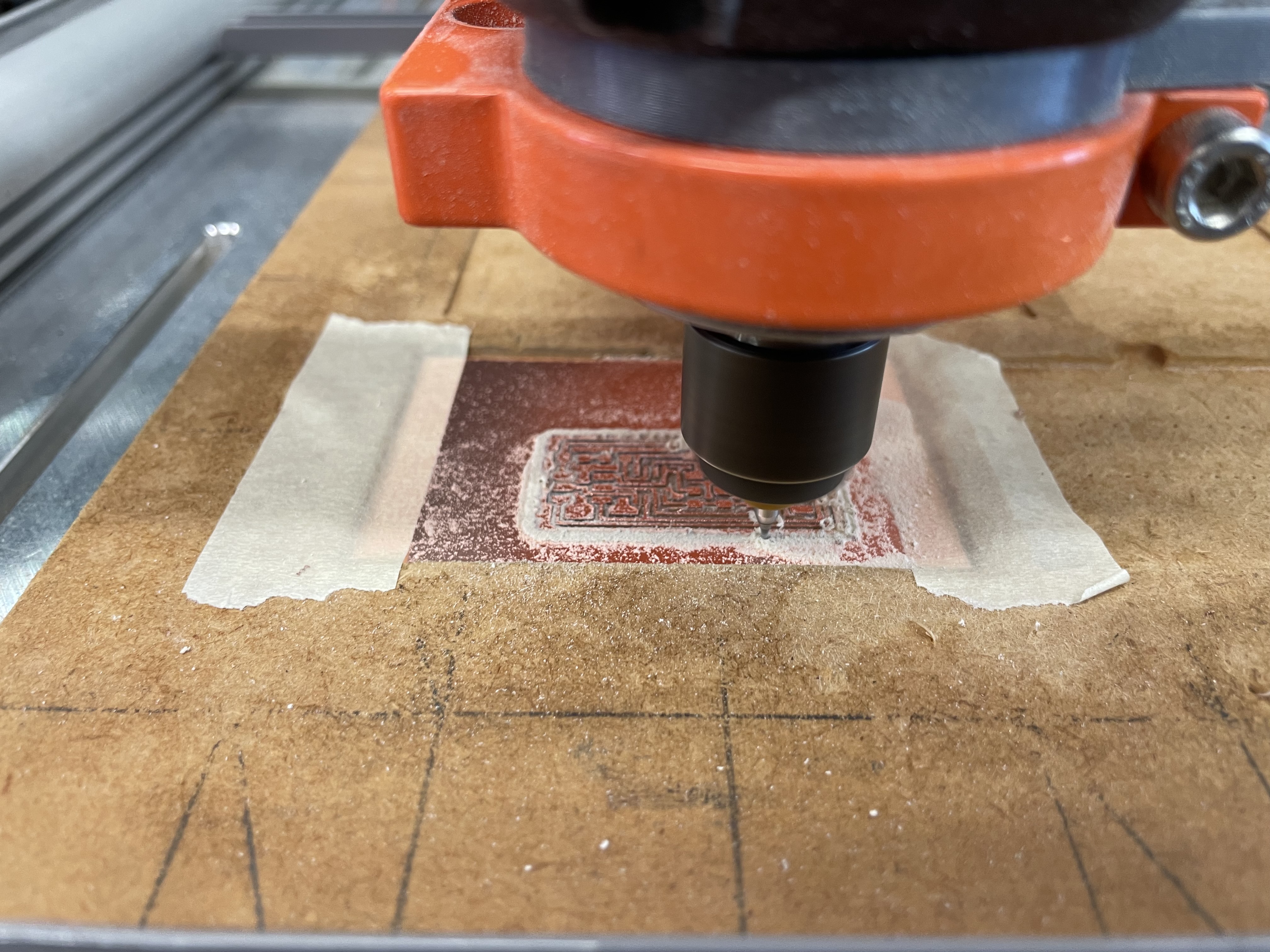
After the gcode was generated, the gcode was then imported into the laptop connected to the stepcraft machine. Then, after setting up the endmill and the stepcraft machinne, the milling process begins.
Slow mo video of the ISP being milled.
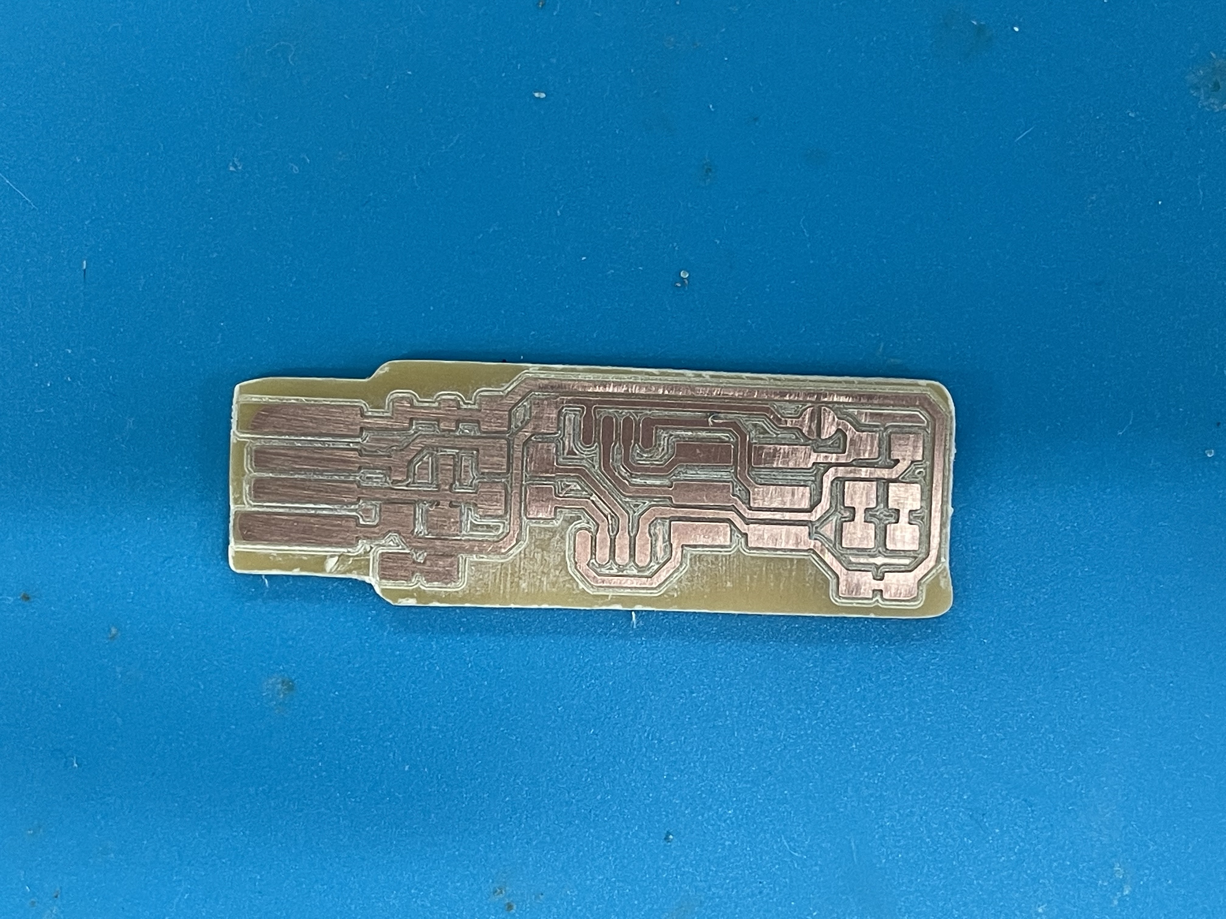
As this is my first time milling a PCB, i was quite afraid that the cut would not work out. Unfornately, that turned out to be true as the traces were too thin to be soldered on, which made me to have to recut.
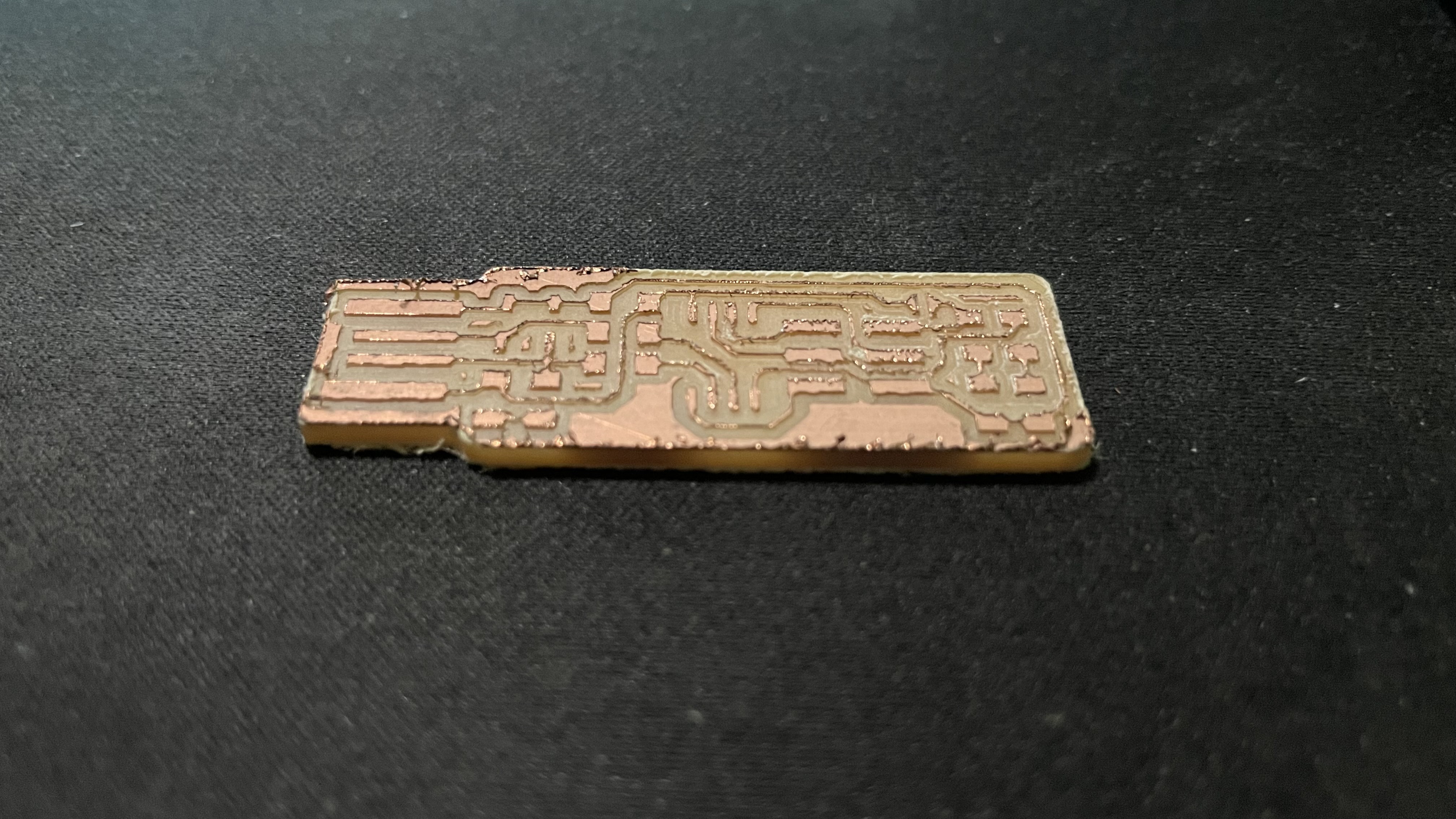
The next cut turned out better as I was able to find and use a better endmill to mill the pcb with. The endmill was sharper which caused the traces to be much cleaner.
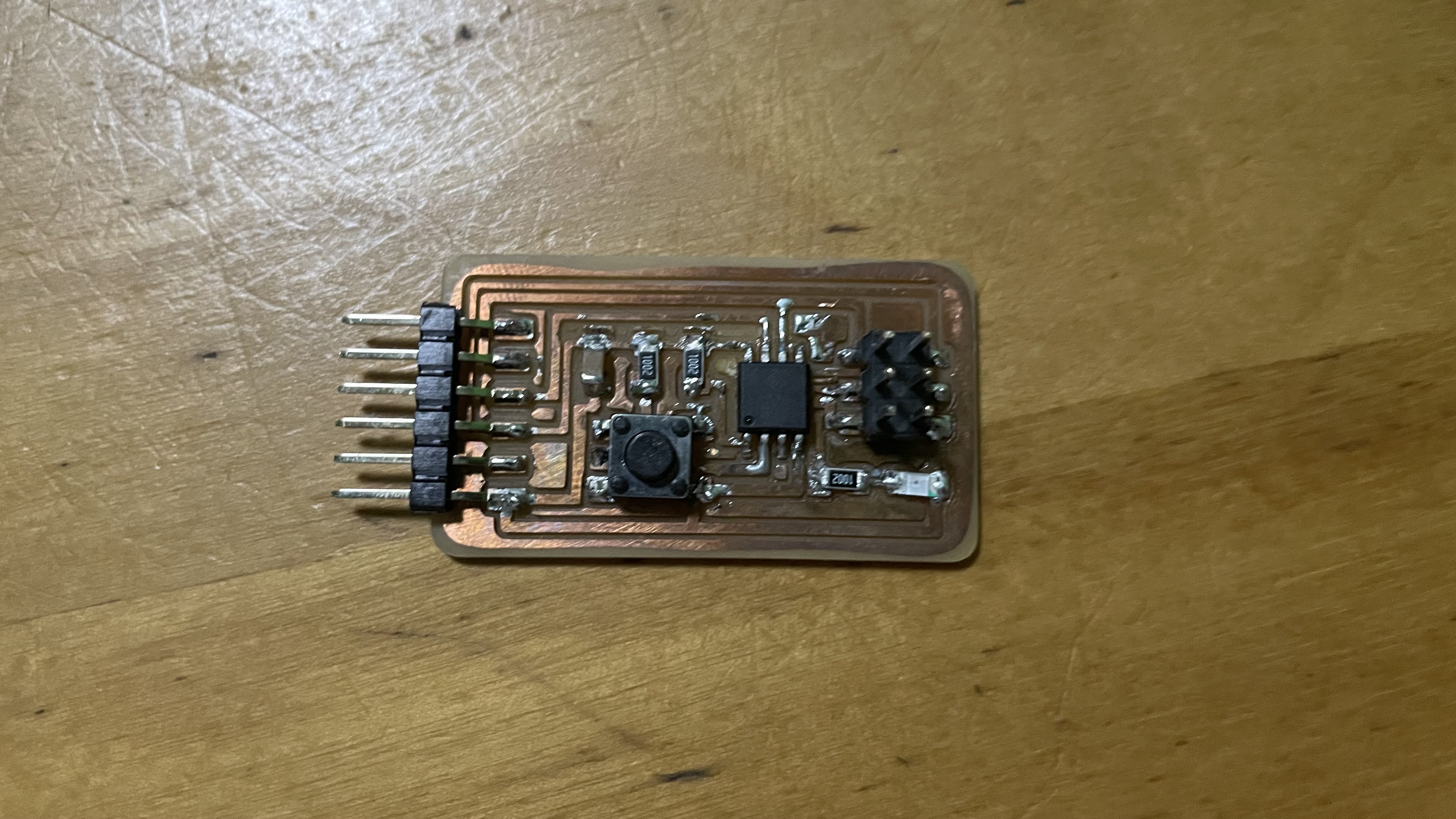
Soldering the components
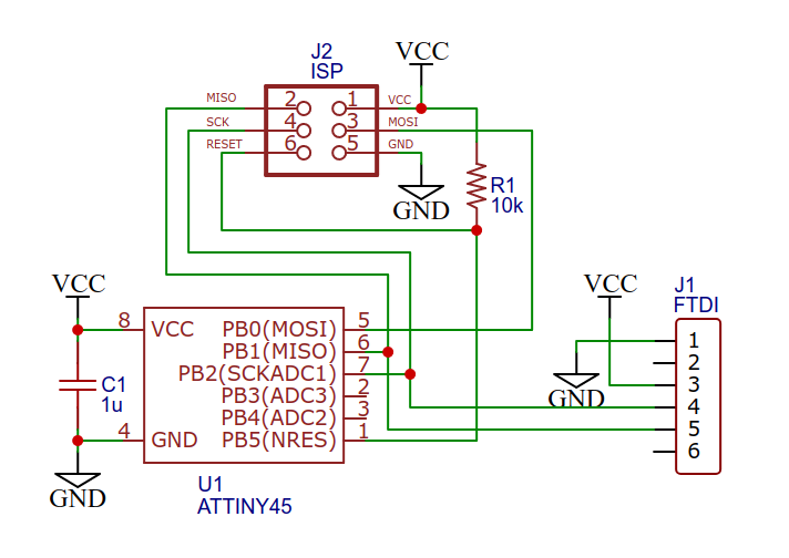
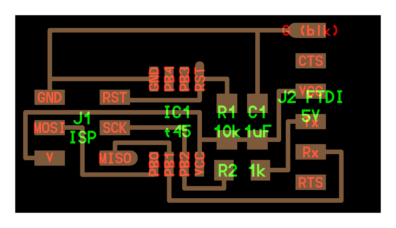
After the board was milled out, it was time to solder the components onto the board. The components used in the board follows this schematic.
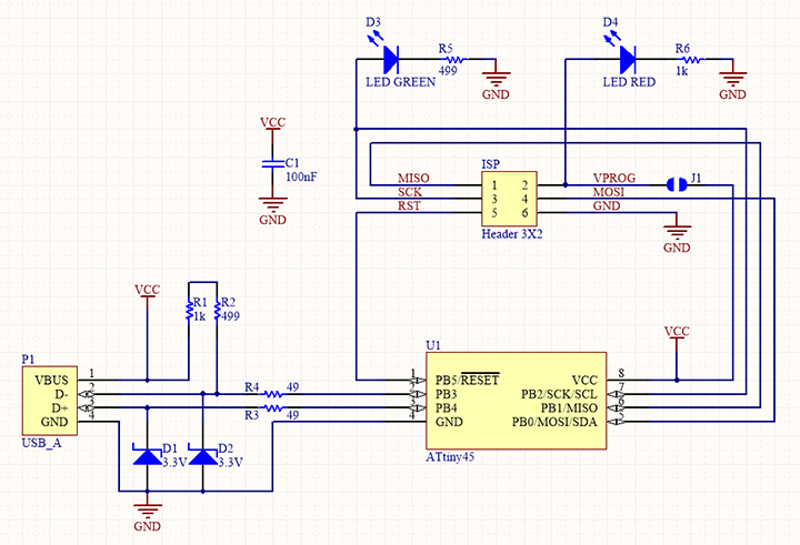
The components that were used include:
- ATtiny85 x 1
- 1kΩ resistor x 2
- 499Ω resistor x 2
- 49Ω resistor x2
- 3.3v zener diode x2
- Red LED x 1
- Green LED x 1
- 100nF capacitor x 1
- 2x3 pin ISP header x 1
- 6mm switch x 1
As the components were already provided in the fablab, the only crucial thing that I needed to do was to solder the components on as neatly as possible. This was also one of my first times soldering, especially using SMD components on such a small board, so I knew I had to be extra careful.
insert image here
After a few tries and large amount of concentration, I finally finished soldering the components onto the board.
Setting up board as ISP Programmer
The following software are needed: GIT for windows Atmel GNU Toolchain GNU make avrdude Zadig
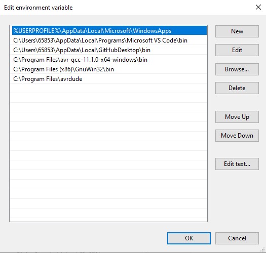
In order to start, the first thing that we need to do is to change some things within the environment variables. Go to System Properties, then Environment variables.
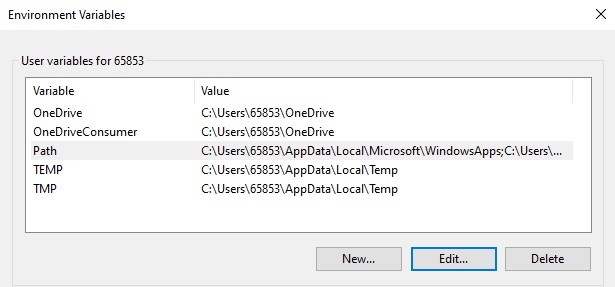
Next, we have to go into environment variables -> PATH, then edit it to add 3 new paths:
C:\Program Files\avrdude
C:\Program Files\avr-gcc-10.1.0-x64-windows\bin
C:\Program Files (x86)\GnuWin32\bin
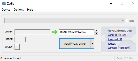
Next, we have to download the necessary drivers. Using Zadig, download and install "libusb-win32" driver for the programmer.
Echo Hello World Boards
Task: To redraw an echo hello-world board
- add (at least) a button and an LED (with current limiting resistor)
- check the design rules (ERC, DRC)
- make it
- test it
Autodesk Eagle
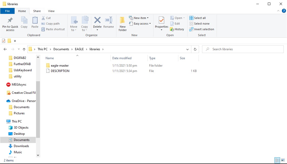
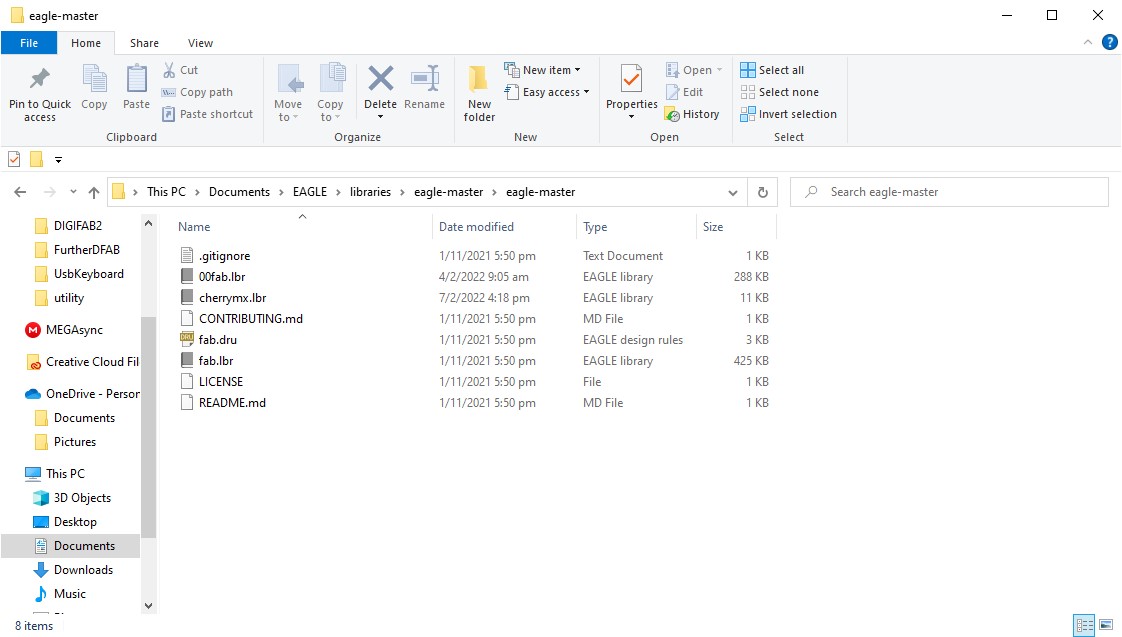
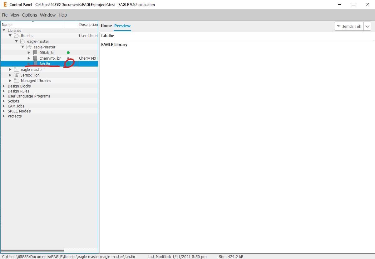
After Eagle was installed, the next thing we needed to do was to add the Fablab EAGLE Library, which will contain the components that we have and will use in the Fablab. In order to download and add the library, we first need to download the zip file, unzip it and move the contents into the eagle library folder.
For the assignment, we had a choice to make a hello board using 3 different types of ATTiny Microcontrollers. I chose to use the ATTiny45/85.
This is the schematic of the Hello Board that i followed.
After creating a new project and schematic, the schematic workspace showed up. This was where i had to add in and connect components for my Hello Board.
To add components to the workspace, click on the Add Part option located at the toolbar on the left side.
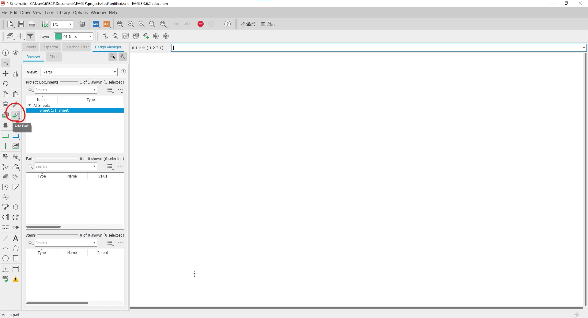
Ensure that the Fablab EAGLE Library is enabled at first before entering the parts panel.
After clicking on add part, all the installed and enabled libraries should show up in a panel, with different components in each library to choose from.
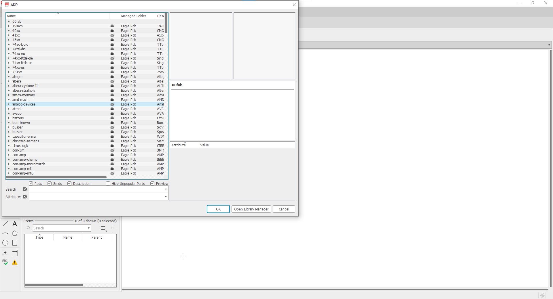
Search for components in the search bar below, in this case I am looking for the ATtiny45, therefore i just input in the search bar *ATtiny45*
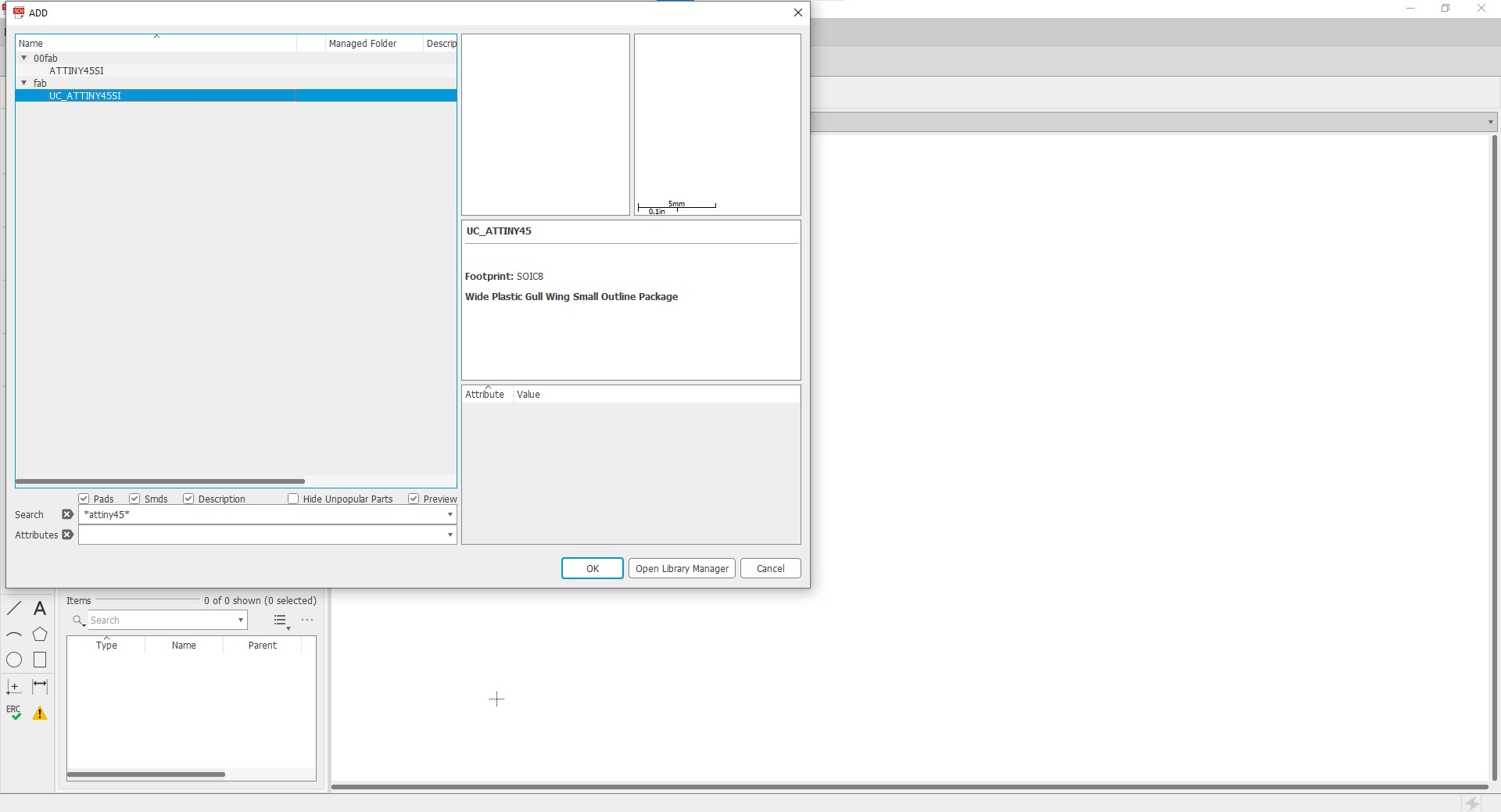
Next, simply click "OK" and click anywhere within the workspace to place the component down. Do the same for every other part that is needed.
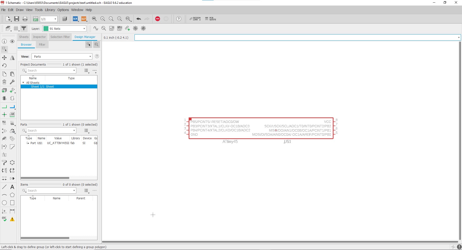
After adding all the components down, we will now need to connect them with wires. By going to the toolbar on the left side again, click on "Net", which is a tool to add wires.
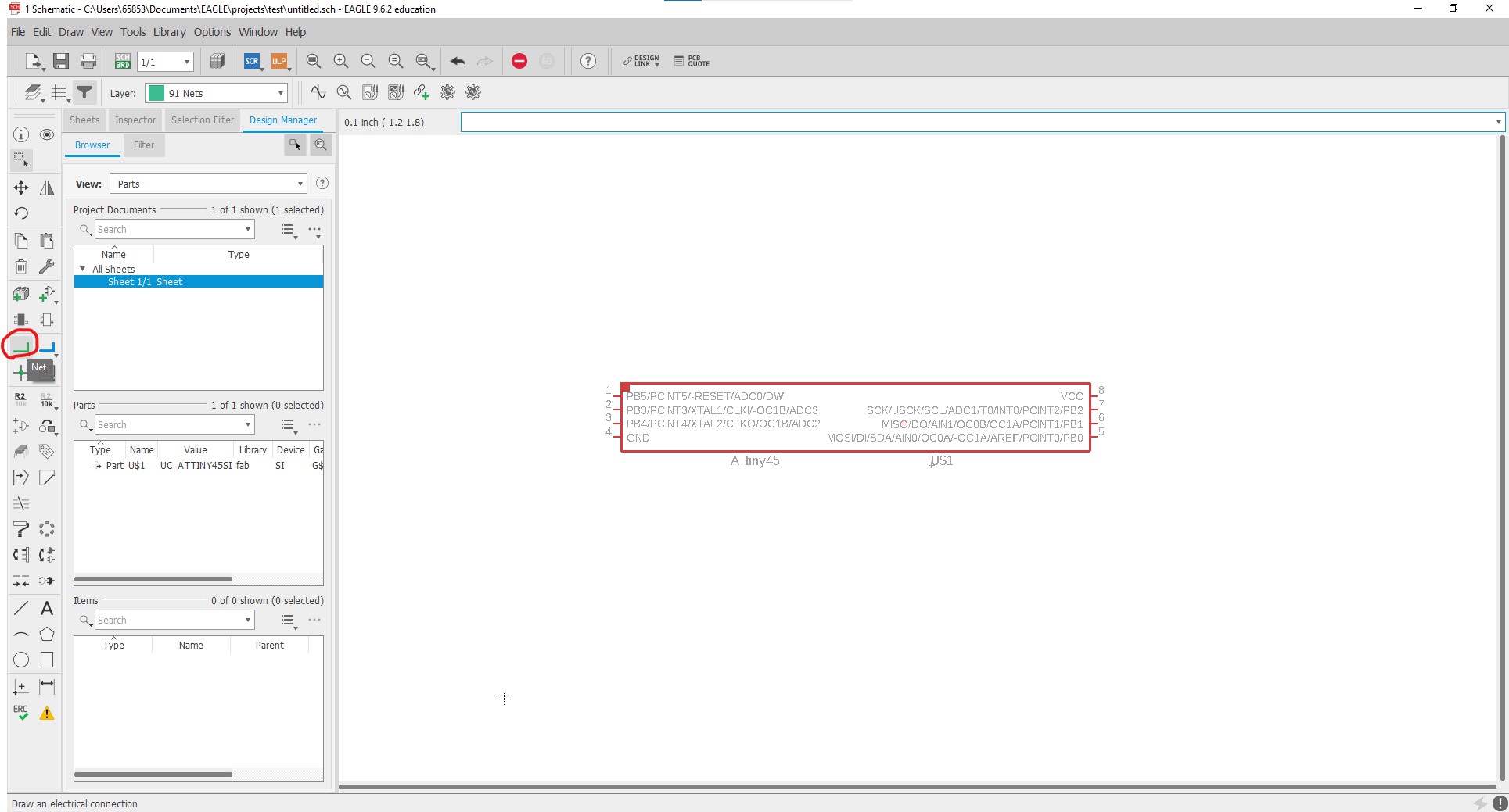
To connect to components together, simply click on one connection point of a component using the Net tool and drag it onto the other point. After connecting all the components together, my schematic turned out like this.
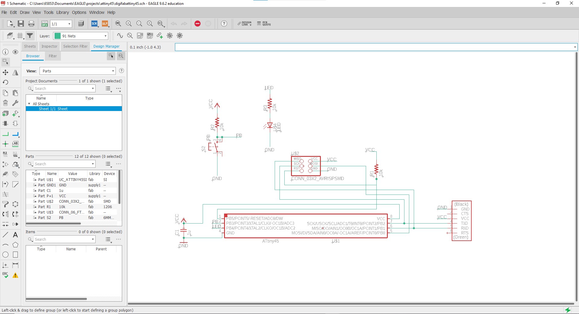
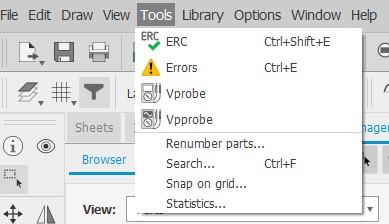
Before I could move on to doing the physical traces of the board, an ERC(Electrical Rule Check) is done to ensure that there is no error in the connections of the circuit. The ERC is located under "Tools" at the top bar.
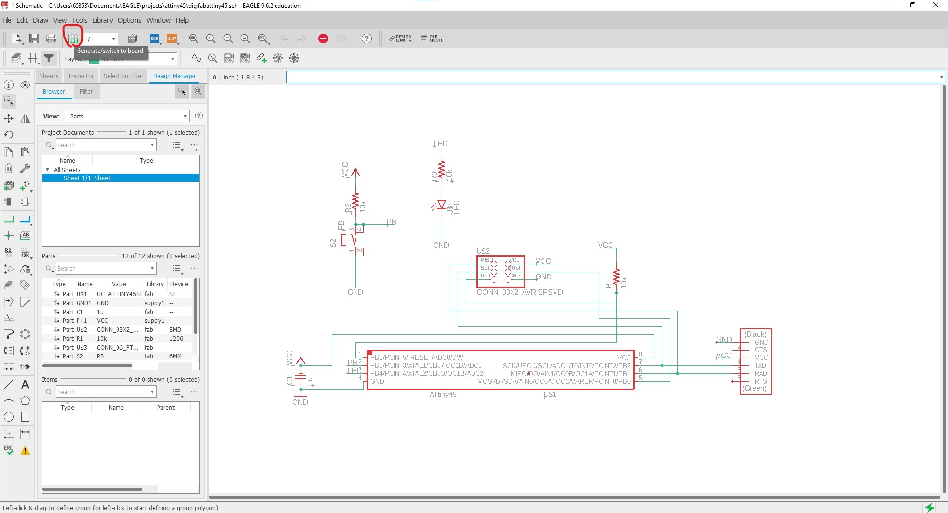
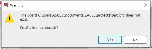
Once the ERC is done, I can now move onto configuring the physical board layout, which is done by clicking on the switch to board/schematic button. If no board was created previously, the system will prompt if a new board was to be created off the current schematic.
After that, Eagle would automatically bring forward the Board workspace. This is where adjustments to the physical board were to be made.
The board layout I would be following is the one that was provided by the lecturer.
When the new board was created, the components would already be laid out at the corner of the workspace. I just simply needed to drag in the components and arrange them to my liking. In order to connect the components together here, I would need to use the "Route Airwire" tool to place down wires.
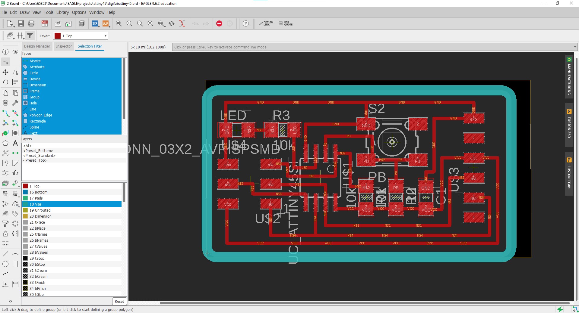
After all the connections were made, the board turned out like this.
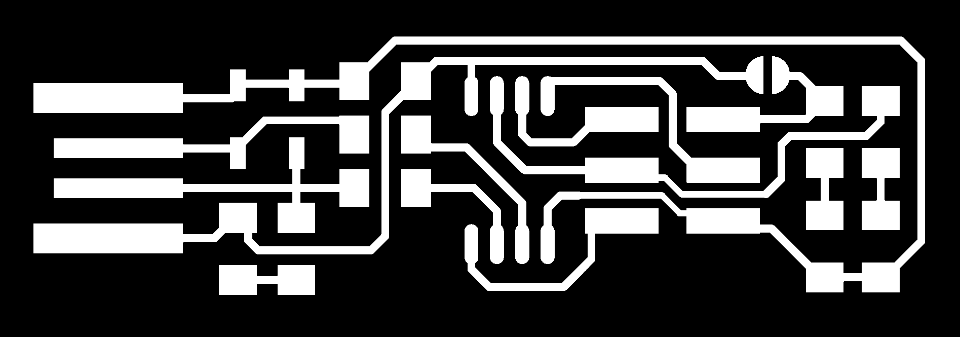
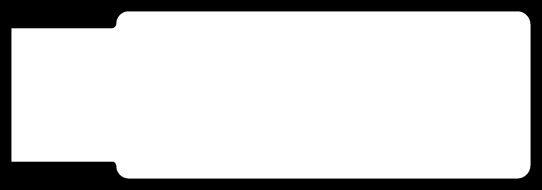
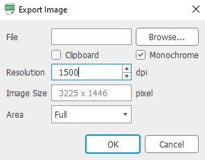
Next, I had to export the traces of the board into an image in order to convert into gcode for the machine to recognise. Before I did that, I ensured that only the top layer is shown, so that only the traces would be exported. I also did the same for the board outline.
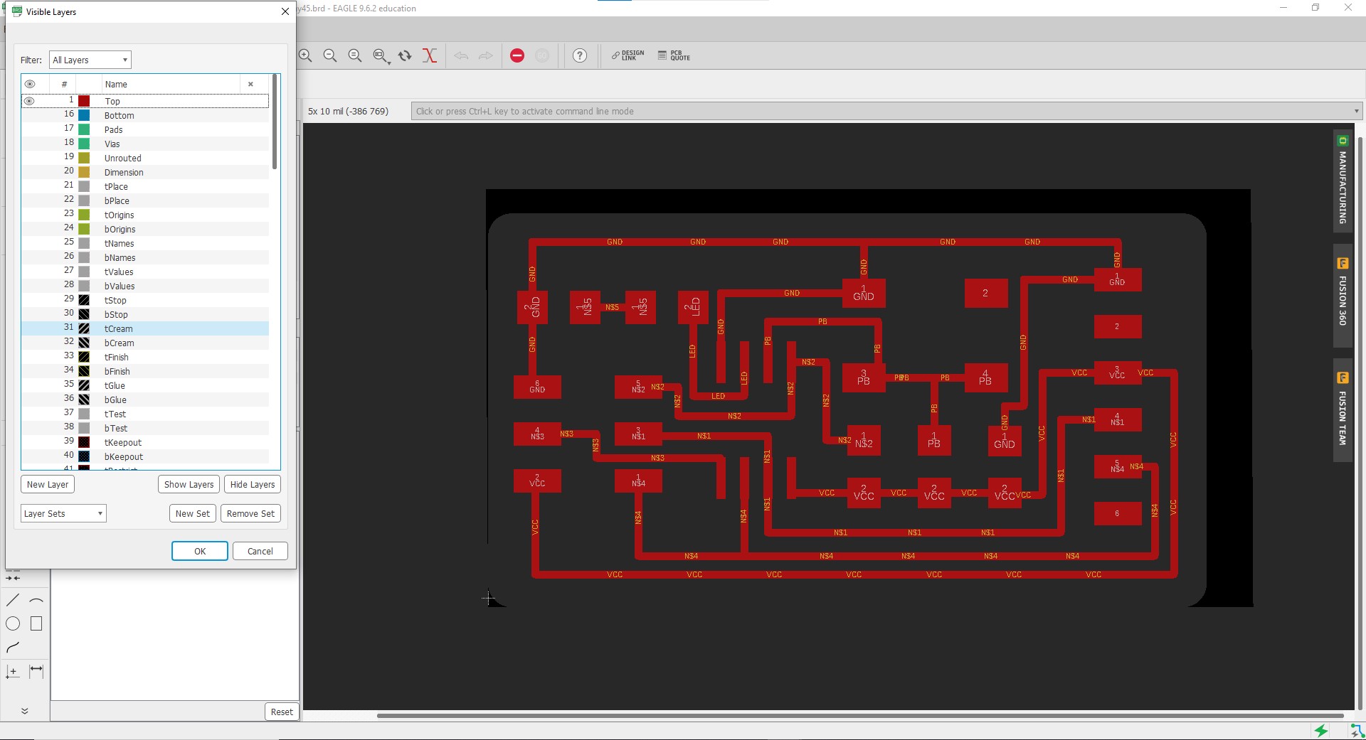
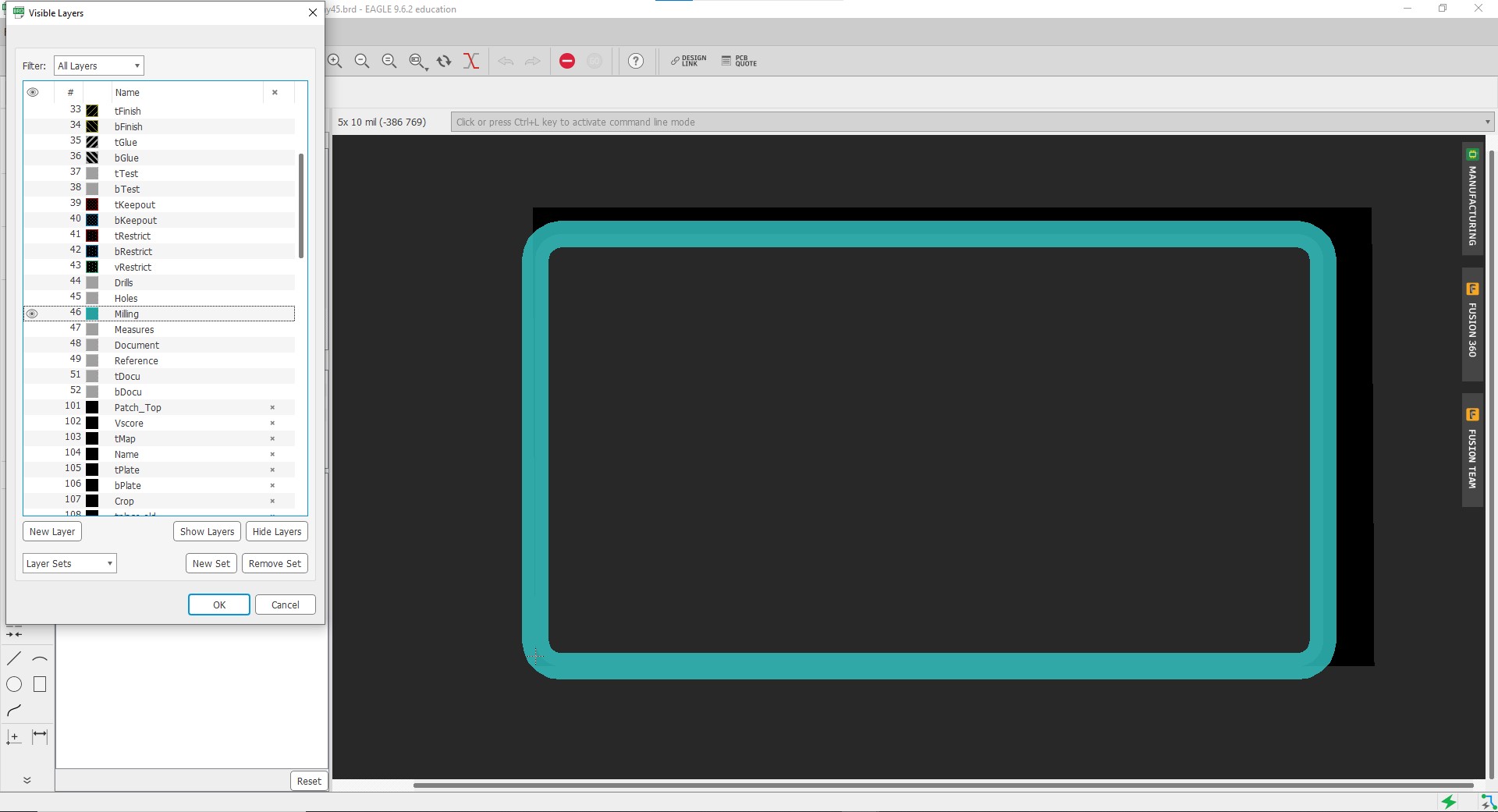
When exporting the image, ensure that the resolution is 1500 dpi and the monochrome option is checked as well.
After export, the images turned out like this.
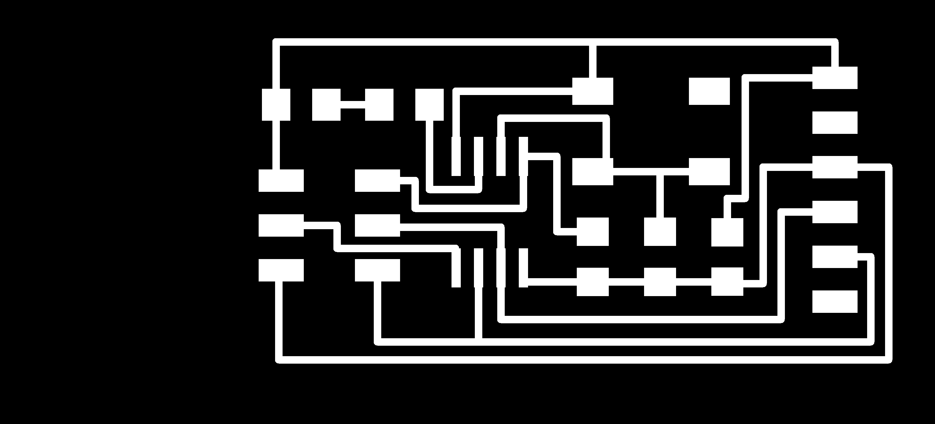

After putting the image through mods and generating the gcode, the board was ready to be milled.
This is how the Hello Board looks like after soldering the components on.
With that, the Hello Board is complete. Some things that I would definitely improve on is the soldering. A lot of the pins had way too much solder than needed and that caused it to look less nice, as well as increased the risk of having a short connection. Next time, I would try to use as little solder as possible.